Purpose
The RT9468 is a switch-mode single cell Li-Ion/Li-Polymer battery charger for portable applications. It integrates a synchronous PWM controller, power MOSFETs, input current sensing and regulation, high-accuracy voltage regulation, and charge termination. The charge current is regulated through integrated sensing resistors. The RT9468 also features USB On-The-Go (OTG) support. The RT9468 integrates an easy-to-use direct charge function, simply driving an external MOSFET to enable a direct charge path, as well as over-voltage protection, over-current protection, and watchdog functions. This document explains the function and use of the RT9468 evaluation board (EVB), and provides information to enable operation, modification of the evaluation board and circuit to suit individual requirements.
Introduction
General Product Information
The RT9468 is a switch-mode single cell Li-Ion/Li-Polymer battery charger for portable applications. It integrates a synchronous PWM controller, power MOSFETs, input current sensing and regulation, high-accuracy voltage regulation, and charge termination. The charge current is regulated through integrated sensing resistors. The RT9468 also features USB On-The-Go (OTG) support. The RT9468 integrates an easy-to-use direct charge function, simply driving an external MOSFET to enable a direct charge path, as well as over-voltage protection, over-current protection, and watchdog functions.
Product Feature
- Direct Charge with Over-Voltage Protection, Over-Current Protection and Watchdog
- High Efficiency 5A, 1.5MHz Switching Charger with Output Inductor DFE252012F, TOKO
►Charging Efficiency 90.25% at ICHG = 2A
►Charging Efficiency 88.86% at ICHG = 3A
►Charging Efficiency 84.2% at ICHG = 5A
- Synchronous 1.5MHz/0.75MHz Fixed-Frequency PWM Controller with Up to 95% Duty Cycle
- Power Path Management by BATFET Control
- Support High Voltage Input (9V/12V)
- Support High Voltage Input Adapter (Pump Express 1.0/2.0/3.0)
- Support IR Compensation Function from Charger Output to Cell Terminal
- Optimize Input Sourcing Capability to Prevent Overload
►AICR Current Limit Setting via I2C
►ILIM Pin for Current Limit Setting
►Average Input Current Limit Measurement
- Shipping Mode for Battery Leakage Reduction
►Wake Up System, Exit Shipping Mode, and Reset System by Pin
Pin
- Automatic Charging
- Average Input Current Regulation (AICR) : 0.1A to 3.25A in 50mA Steps
- Charge Current Regulation Accuracy : ±7%
- Charge Voltage Regulation Accuracy : ±1% (0 to 85°C)
- Protection for Overall System Considerations
►Thermal Regulation for Current Reduction and Over-Temperature Protection
►Input Over-Voltage Protection
►Input Bad Adapter Protection
►Battery Over-Voltage Protection
- Support ADC Conversion for
►VBUS, VBAT, VSYS, REGN, TS_BAT, IBUS, IBAT,TEMP_JC, TS_BUS, VBATS, IBATS
- INT Output for Communication with Host Through I2C (Watch Dog / Polling Function)
Key Performance Summary Table
|
Key Features
|
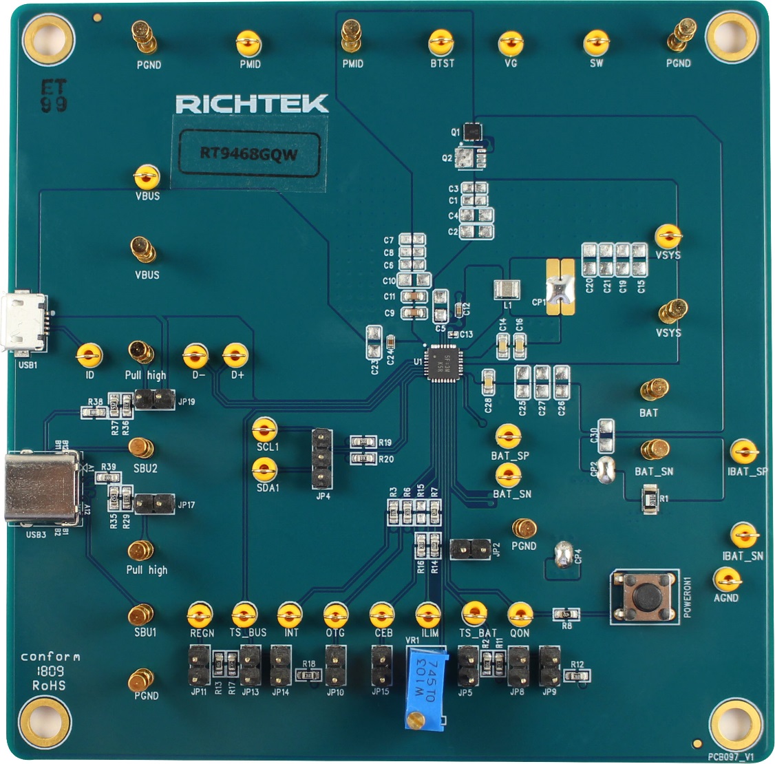
Evaluation Board Number : PCB097_V1
|
|
Input Voltage
|
3.9V to 14V
|
|
Output Voltage
|
3.8V to 5.06V
|
|
Maximum Output Current
|
0A to 5A
|
|
Package Type
|
RT9468GQW, WQFN-32L 4x4
|
Bench Test Setup Conditions
Headers Description and Placement
Carefully inspect all the components used in the EVB according to the following Bill of Materials table, and then make sure all the components are undamaged and correctly installed. If there is any missing or damaged component, which may occur during transportation, please contact our distributors or e-mail us at evb_service@richtek.com.
Test Points
The EVB is provided with the test points and pin names listed in the table below.
|
Test point/
Pin name
|
Signal
|
Comment (expected waveforms or voltage levels on test points)
|
|
VBUS
|
Input
|
Power input.
|
|
D+
|
USB D+ Port
|
Connected to USB receptacle.
|
|
D-
|
USB D- Port
|
Connected to USB receptacle.
|
|
TS_BUS
|
BUS Temperature-Sense Input
|
Connected to a resistor divider for temperature programming. If there is no need for the battery temperature-sense function, a 50kΩ resistor is connected to REGN and another 50kΩ resistor to ground.
|
|
SCL
|
I2C Interface Serial Clock Input
|
Open-drain. An external pull-up resistor is required.
|
|
SDA
|
I2C Interface Serial Data Input/Output
|
Open-drain. An external pull-up resistor is required.
|
|
INT
|
Interrupt output
|
Active-low open-drain. Indicator of the charger/boost event for system processor.
|
|
OTG
|
OTG Boost Mode Enable Control
|
Active-high. Act with OTG_PIN_EN (0x01[1]).
|
|
CEB
|
Charger Enable Input
|
Active-low.
|
|
ILIM
|
Input Current Limit Setting Pin
|
A resistor is connected from ILIM pin to ground to set the maximum input current limit. The actual input current limit is the lower value set through the ILIM pin and IAICR register bits.
|
|
TS_BAT
|
Battery Temperature-Sense Input
|
connected to a resistor divider for temperature programming. If there is no need for the battery temperature-sense function, a 50kΩ resistor is connected to REGN and another 50kΩ resistor to ground.
|
|

|
Internal BATFET Enable Control Input
|
In shipping mode, is pulled Low for the duration of tSHIPMODE (typical 0.9s) to exit shipping mode. is pulled Low for the duration of tSHIPMODE (typical 0.9s) to exit shipping mode.
|
|
IBAT_SN
|
Negative Battery Current Sense
|
Negative battery current sense. Connect a 10mΩ between IBAT_SP.
|
|
IBAT_SP
|
Positive Battery Current Sense
|
Positive battery current sense. Connect a 10mΩ between IBAT_SN.
|
|
BAT_SN
|
Negative Battery Current Sense
|
Connect to battery connect.
|
|
BAT_SP
|
Positive Battery Current Sense
|
Connect to battery connect.
|
|
BAT
|
Battery Connection Node
|
Charging current output node. Internal BATFET is connected between SYS and BAT.
|
|
SYS
|
System Connection Node
|
The internal BATFET is connected between SYS and BAT. Connect a 20µF ceramic capacitor between SYS and ground.
|
|
SW
|
Switch Node
|
Switch node for output inductor connection.
|
|
BTST
|
Bootstrap Capacitor Connection for High-Side Gate Driver
|
Connect a capacitor from BTST to SW to power the internal gate driver.
|
|
REGN
|
Regulated Output Voltage
|
Connect a 4.7µF ceramic capacitor from REGN to GND.
|
|
VG
|
Gate Driver Output
|
Gate driver output for external N-MOSFET.
|
|
PMID
|
PMID
|
Connection point between the reverse blocking MOSFET and the high-side switching MOSFET.
|
|
PGND
|
Power Ground
|
Power ground connection. The exposed pad must be connected to GND and well soldered to a large PCB copper area for maximum power dissipation.
|
Power-Up & Measurement Procedure
1. Connect input power (5 < VBUS < 14V) and input ground to VIN and GND test pins respectively.
2. Connect positive end and negative terminals of VBAT to BAT and BAT_SN test pins respectively.
3. Connect JP11, JP14, JP5 and JP9 let TS_BUS and TS_BAT at normal condition.
Schematic, Bill of Materials & Board Layout
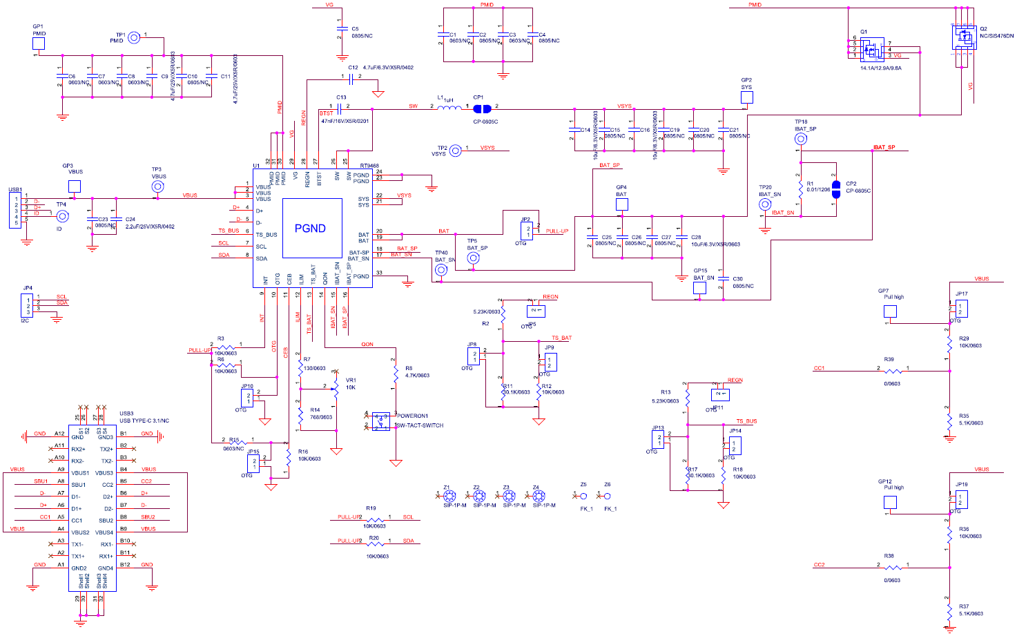
EVB Schematic Diagram
Bill of Materials
|
Reference
|
Qty
|
Part Number
|
Description
|
Package
|
Manufacturer
|
|
C9, C11
|
2
|
GRM188R61E475KE11
|
4.7µF/25V/X5R
|
0603
|
muRata
|
|
C12
|
1
|
GRM155R60J475ME47
|
4.7µF/6.3V/X5R
|
0402
|
muRata
|
|
C13
|
1
|
GRM033R61C473KE84
|
47nF/16V/X5R
|
0201
|
muRata
|
|
C14, C16, C28
|
3
|
GRM185R60J106ME15
|
10µF/6.3V/X5R
|
0603
|
muRata
|
|
C24
|
1
|
GRM155R61E225KE11
|
2.2µF/25V/X5R
|
0402
|
muRata
|
|
L1
|
1
|
DFE252012F-1R0M
|
1µH
|
2.5x2.0mm
|
muRata
|
|
Q1
|
1
|
DMT2004UFDF
|
NMOS
|
2x2x0.6mm
|
DIODES
|
|
U2
|
1
|
RT9468GQW
|
Switching Charger
|
WQFN-32L 4x4
|
Richtek
|
|
R1
|
1
|
WR06X5231FTL
|
5.23k/0603
|
1206
|
WELLCOMP TECHNOLOGY
|
|
R2, R13
|
2
|
WR06X1002FTL
|
10k/0603
|
0603
|
WALSIN
|
|
R3, R6, R12, R16, R18, R19, R20, R29, R36
|
9
|
WR06X1300FTL
|
130/0603
|
0603
|
WALSIN
|
|
R7
|
1
|
WR06X4701FTL
|
4.7k/0603
|
0603
|
WALSIN
|
|
R8
|
1
|
WR06X3012FTL
|
30.1k/0603
|
0603
|
WALSIN
|
|
R11, R17
|
2
|
WR06X7680FTL
|
768/0603
|
0603
|
WALSIN
|
|
R14
|
1
|
WR06X5231FTL
|
5.23k/0603
|
0603
|
WALSIN
|
|
R35, R37
|
2
|
WR06X5101FTL
|
5.1k/0603
|
0603
|
WALSIN
|
|
R38, R39
|
2
|
WR06X000 PTL
|
0/0603
|
0603
|
WALSIN
|
|
USB1
|
1
|
|
SIP-5P
|
USB-MICRO-TCU-S60M
|
|
|
USB3
|
1
|
121U-3CST-09CR
|
USB TYPE-C 3.1
|
9.87x9.75mm
|
JEM (建舜電子)
|
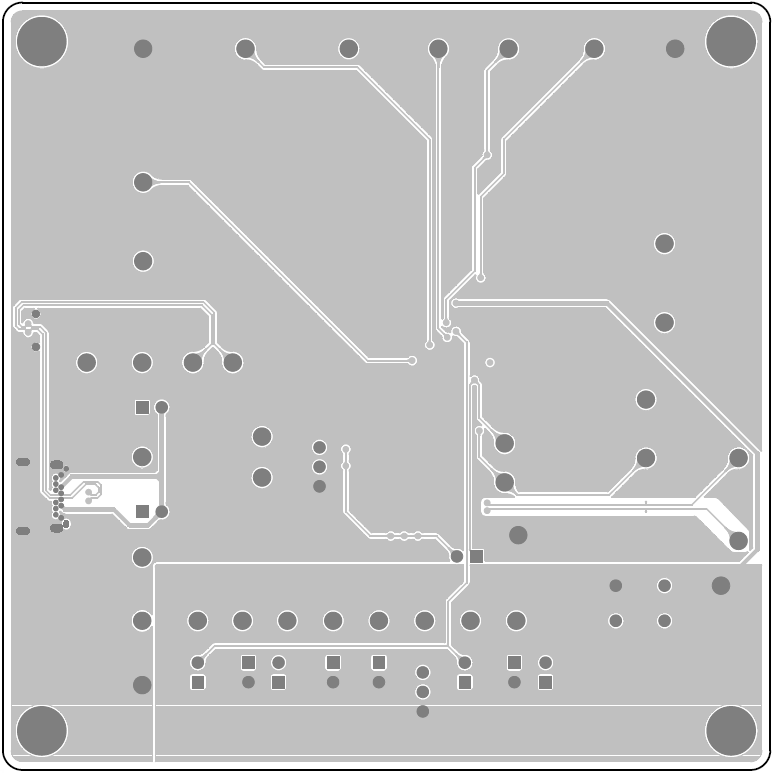
PCB Layout
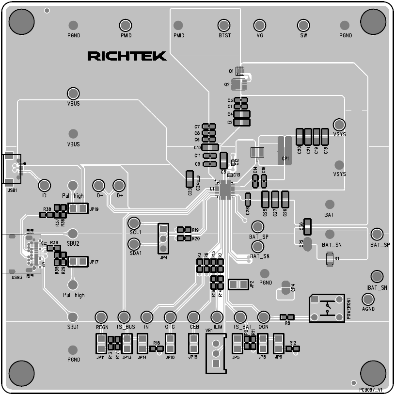
Top View (1st layer)
PCB Layout—Inner Side (2nd Layer)
PCB Layout—Inner Side (3rd Layer)
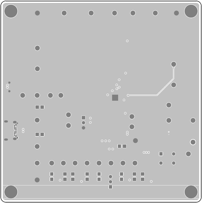
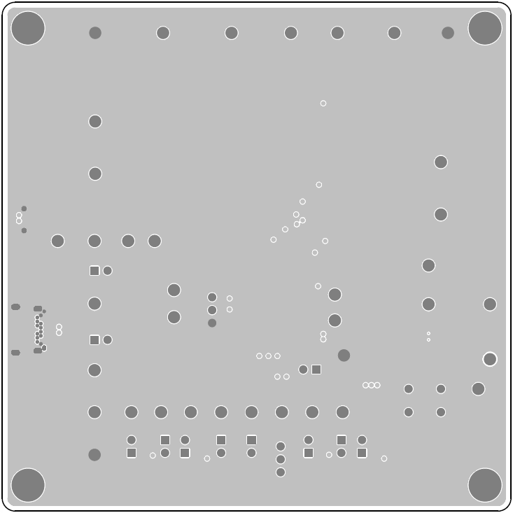
Bottom View (4th Layer)